

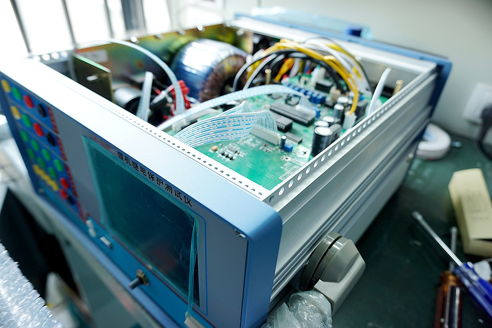
An immersion gold PCB is one of the most widely used printed circuit board surface finishes in modern electronics manufacturing. Known for its flat surface, excellent solderability, and long shelf life, immersion gold has become a preferred choice for fine-pitch components, high-density designs, and applications requiring consistent electrical performance. As electronic devices continue to become smaller and more complex, immersion gold PCBs play a critical role in ensuring assembly reliability and long-term durability.
This article explores what an immersion gold PCB is, how it is manufactured, its advantages, applications, and why working with the right immersion gold PCB manufacturer is essential for quality results.
What Is an Immersion Gold PCB?
An immersion gold PCB is a circuit board finished with an ENIG surface treatment, which stands for Electroless Nickel Immersion Gold. This process deposits a layer of nickel onto the exposed copper pads, followed by a thin layer of gold applied through an immersion process.
The nickel layer acts as a barrier that prevents copper diffusion, while the gold layer protects the nickel from oxidation and ensures excellent solderability. Unlike some other finishes, immersion gold provides a very flat and uniform surface, making it ideal for advanced PCB assembly processes.
Immersion gold PCBs are commonly used in applications that involve fine-pitch ICs, BGAs, and high-reliability electronic systems.
Structure and Characteristics of Immersion Gold PCB
The defining feature of an immersion gold PCB is its multilayer surface finish. The nickel layer typically ranges from 3 to 6 microns in thickness, providing mechanical strength and wear resistance. The immersion gold layer is much thinner, usually around 0.05 to 0.1 microns, but it plays a crucial role in oxidation protection and solder joint quality.
This combination results in a surface that is smooth, corrosion-resistant, and compatible with both lead-free and leaded soldering processes. Immersion gold PCBs also support wire bonding in certain applications, adding to their versatility.
Immersion Gold PCB Manufacturing Process
The manufacturing process of an immersion gold PCB begins after standard PCB fabrication steps such as imaging, etching, drilling, and solder mask application. Once the copper pads are exposed and cleaned, the board enters the ENIG process.
Electroless nickel is deposited first through a chemical reaction that does not require an external power source. This ensures uniform coverage even on complex pad geometries. After the nickel layer is formed, the board is immersed in a gold solution where a thin gold layer replaces a portion of the nickel surface.
The process is carefully controlled to ensure consistent layer thickness and prevent defects. Final inspection and testing verify surface quality, solderability, and electrical performance.
Advantages of Immersion Gold PCB
One of the primary advantages of an immersion gold PCB is excellent solderability. The gold layer protects the nickel surface until soldering, resulting in strong and reliable solder joints. This is especially important for fine-pitch and high-density components.
Another major benefit is surface flatness. Immersion gold provides a planar surface that supports precise component placement, reducing the risk of assembly defects. This makes it ideal for automated assembly lines and advanced packaging technologies.
Immersion gold PCBs also offer long shelf life. Unlike some surface finishes that oxidize quickly, immersion gold boards can be stored for extended periods without compromising solderability.
Immersion Gold PCB vs Other Surface Finishes
Compared to HASL finishes, immersion gold PCBs offer significantly better flatness and are more suitable for fine-pitch designs. HASL can create uneven surfaces that may cause issues with small components.
When compared to OSP finishes, immersion gold provides superior durability and storage life. OSP is more cost-effective but less robust for long-term storage or multiple soldering cycles.
ENEPIG and hard gold finishes offer additional features such as improved wire bonding or wear resistance, but immersion gold remains a balanced choice in terms of performance, cost, and versatility for many applications.
Applications of Immersion Gold PCB
Immersion gold PCBs are widely used across various industries. In consumer electronics, they are commonly found in smartphones, tablets, and wearable devices where compact designs and fine-pitch components are standard.
Telecommunications equipment relies on immersion gold PCBs for stable signal transmission and reliable assembly. Industrial control systems and automotive electronics benefit from their durability and consistent solder joint quality.
Medical devices also use immersion gold PCBs due to their reliability, cleanliness, and compatibility with high-precision components.
Quality Standards and Testing for Immersion Gold PCB
Quality control is critical in immersion gold PCB production. Manufacturers conduct thickness measurements to ensure proper nickel and gold layer deposition. Visual inspection checks for surface defects such as black pad, discoloration, or uneven coating.
Solderability testing verifies joint strength and wetting behavior during assembly. Electrical testing ensures circuit integrity and insulation performance. A professional manufacturer follows strict process controls to avoid common ENIG-related issues.
How to Choose the Right Immersion Gold PCB Manufacturer
Selecting the right immersion gold PCB manufacturer is essential for achieving consistent quality and reliable performance. Experience with ENIG processes is a key factor, as precise chemical control is required to prevent defects.
Manufacturing capability should include advanced inspection systems and strict quality management standards. A reliable manufacturer will also provide technical support, helping optimize pad design and surface finish selection for specific applications.
Lead time flexibility, communication transparency, and stable production capacity are also important when choosing a long-term manufacturing partner.
Future Trends in Immersion Gold PCB Technology
As electronic products continue to shrink and increase in complexity, demand for immersion gold PCBs is expected to grow. Advancements in ENIG chemistry and process control are improving reliability and reducing defect risks.
Sustainability is also influencing surface finish development, with manufacturers focusing on environmentally friendly chemical processes and waste reduction. These trends ensure immersion gold PCBs remain a key solution for advanced electronics manufacturing.
Conclusion
An immersion gold PCB is a proven and reliable surface finish solution for modern electronic designs that demand excellent solderability, flatness, and long-term stability. From consumer electronics to industrial and medical applications, immersion gold PCBs deliver consistent performance and assembly reliability.
To ensure high-quality results and dependable production, partnering with an experienced immersion gold PCB manufacturer is the best way to turn complex PCB designs into reliable, production-ready electronic products.

